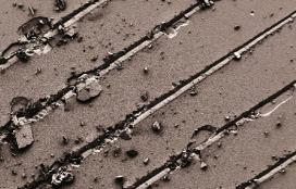
Thin films and coatings (from a few nm to about 1 µm thick) need to be optimised both in the mechanical properties and tribological performance.Typically, this is done with a combination of indentation and scratch tests.Conventional scratch test conditions are not appropriate for these types ofmaterials as they were developed for testing thicker coatings. Instead thenano-scratch & wear module can provide what is needed. Figure 1: Ramped scratches to 500 mN show brittle fracture of 1.5 µm TiFeN films on Si at high load.
薄膜和涂层(从几纳米到约1微米厚)在机械性能和摩擦学性能方面都需要优化。通常,这是通过压痕和划痕测试的组合来完成的。传统的划痕试验条件不适用于这些类型的材料,因为它们是为测试较厚的涂层而开发的。相反,纳米划痕和磨损模块可以提供所需的东西。
图1:500 mN的倾斜划痕显示,在高负载下,Si上1.5 μ m的TiFeN薄膜脆性断裂。
How it works
The sample to be tested is moved perpendicular to the scratch probe whilstthe contact is either held constant or ramped at a user-defined rate.Throughout the test the probe penetration depth and tangential (frictional)load are continuously monitored. Single and multi-pass tests are possible. Multi-pass tests allow the investigation of nano-wear and micro-wear.
The Nano-Scratch & Wear module has found many applications in sectorsas diverse as optical, microelectronics, polymer/biomaterial, and tribologicalcoatings. It is available as a stand alone instrument (nano-scratchtester) or as an option for the NanoTest Vantage platform.
运作原理
待测样品垂直于划痕探针移动,同时接触保持恒定或以用户定义的速率倾斜。在整个测试过程中,探针穿透深度和切向(摩擦)载荷被持续监测。可以进行单次和多次测试。多道次试验可以研究纳米磨损和微磨损。
纳米划痕和磨损模块在光学、微电子、聚合物/生物材料和摩擦学涂层等领域得到了广泛应用。它可以作为一个独立的仪器(纳米划痕仪)或作为NanoTest Vantage平台的一个选项。
Ramped scratch, corrected for baseline sampletopograp

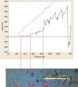
Figure 2 shows a scratch test with 3 µm end radius probe scanning over a 150 µm track at a scan speed of 2 µm/s.
A pre-scratch scan was carried out using an ultra low contact force inorder to assess baseline sample topography.
The red line shows the on-load probe depth, which represents elastic and plastic depth. After 20 µm the load is ramped at 2.5 mN/s.
The black line shows the residual (plastic) depth once the scratch loadhas been removed. This has been corrected for initial sample topography.
The frictional force on the indenter can be recorded throughout theexperiment.
斜坡划痕,根据基线样本地形进行校正
图2显示了用3µm末端半径探针在150µm轨道上扫描的划痕测试,扫描速度为2µm/s。
使用超低接触力进行预刮擦扫描,以评估基线样品地形。
红线为有载探头深度,表示弹塑性深度。在20µm后,负载上升到2.5mN/s。
黑线显示一旦划痕载荷被移除后的残留(塑料)深度。这已经对初始样品地形进行了校正。
压头上的摩擦力可以在整个实验过程中记录下来。
Micro-scratch Testing
The 30 N high load head can be used across the full load range formicro-scratch and micro-wear testing. The frictional force on the indenter canalso be recorded throughout the entire load range.
This high load scratch capability is available on NanoTest Vantage and NanoTest Xtreme instrumentsequipped with the high load head.
Check out our high temperature micro-scratch and impact testing tech note whichdescribes case studies that combine the proven NanoTest high temperaturecapability with micro-scale scratch and impact tests on hard, wear-resistantcoatings.
Micro-scratch 测试
30 N高负载头可用于全负载范围的微划痕和微磨损测试。压头上的摩擦力也可以在整个负载范围内记录。
这种高负载划痕能力可用于配备高负载头的NanoTest Vantage和NanoTest Xtreme仪器。
请查看我们的高温微划痕和冲击测试技术说明,其中描述了将经过验证的NanoTest高温可重性与硬质耐磨涂层的微划痕和冲击测试相结合的案例研究。
